Intro Link to heading
I needed to extract firmware from a locked nRF52840, a microcontroller from Nordic’s nRF52 series that’s common in IoT devices like smartwatches, game controllers, and sensors. These chips are small but powerful, with ARM processors, wireless, flash, NFC, and more. Bypassing locks like this matters for security researchers testing IoT vulnerabilities, but it also shows why chipmakers need stronger protections. Normally, you’d connect a debug probe and dump the flash, but this chip’s debug port was disabled.
Fortunately, others have already explored this chip and found it vulnerable to voltage glitching. I decided to follow that path and try to reproduce Limited Result’s experiment.
While this post isn’t breaking new ground, my take might help someone else facing the same challenge.
Here’s what I set out to do:
- Figure out how the debug lock works.
- Try to bypass the debug lock by reproducing the experiment on a development board.
- Remove the chip from the real target device, solder it onto the development board, and run the attack again to finally extract the firmware.
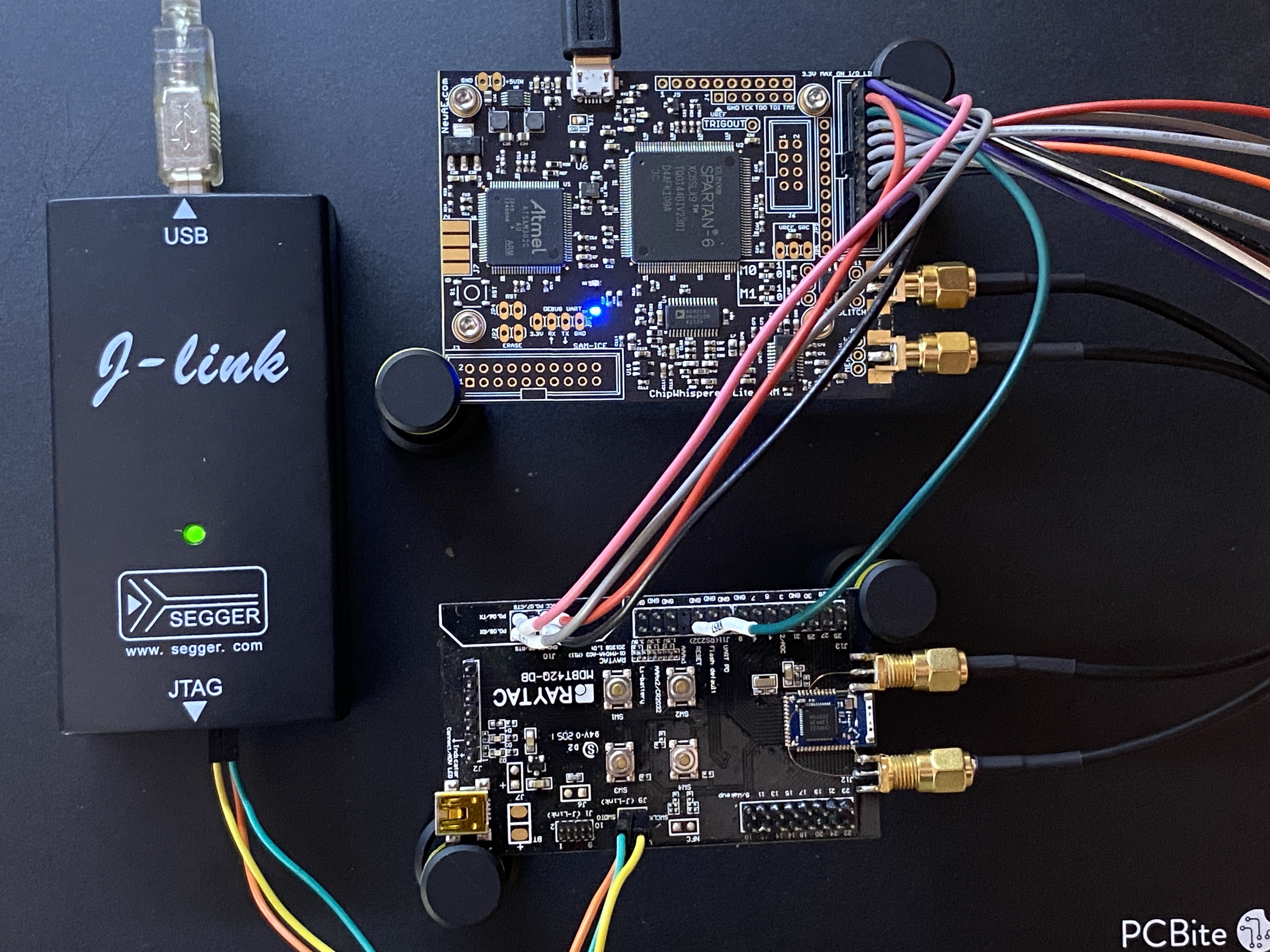
Using a development board let me isolate the chip from the real device’s circuit, avoiding power line issues with other components. This made testing cleaner, and once it worked, I could swap in the actual chip, which is the same model. I used a MDBT42Q-DB-32 Demo Board containing Raytac’s MDBT42Q-512KV2 module, which is basically an nRF52840 paired with an antenna and some passives.
Some reports suggest a newer revision of the chip may address the vulnerability, but I haven’t confirmed this. My device uses the older, vulnerable revision.
The Debug Lock: APPROTECT Link to heading
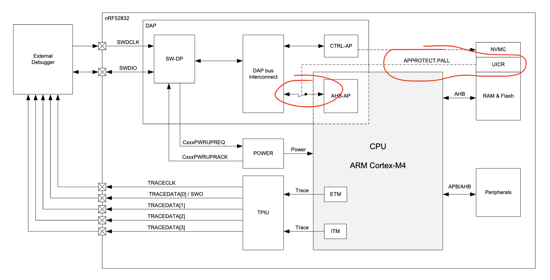
APPROTECT stands for access port protection, a security feature that locks down the chip’s debug interface to prevent unauthorized access.
From the nRF52840 datasheet:
Access Port Protection blocks the debugger from read and write access to all CPU registers and memory-mapped addresses when enabled.
The nRF52 SoC includes a debug and trace system that allows access to memory and the CPU via the SWD protocol. This is managed internally by the AHB-AP (Advanced High-performance Bus Access Port).
As shown in the image below, there’s a switch controlled by the UICR.APPROTECT register that can block access to the AHB-AP. When APPROTECT is enabled, only the CTRL-AP remains accessible. The CTRL-AP can restore APPROTECT, but erases all data in the process.
What Does This Look Like in Practice? Link to heading
Starting with an unprotected device (APPROTECT not enabled), using OpenOCD and a debug probe connected to the development board, I got the following:
$ openocd -f interface/stlink.cfg -f target/nrf52.cfg
[...]
Info : STLINK V2J33S7 (API v2) VID:PID 0483:3748
Info : Target voltage: 3.207828
Info : nrf52.cpu: hardware has 6 breakpoints, 4 watchpoints
Info : starting gdb server for nrf52.cpu on 3333
Info : Listening on port 3333 for gdb connections
Just to understand OpenOCD output, I disconnected the SWD line and tried to connect again. Here’s what I got:
$ openocd -f interface/stlink.cfg -f target/nrf52.cfg
[...]
Info : STLINK V2J33S7 (API v2) VID:PID 0483:3748
Info : Target voltage: 3.210430
Error: init mode failed (unable to connect to the target)
And finally, I enabled APPROTECT and tried again:
$ openocd -f interface/stlink.cfg -f target/nrf52.cfg
[...]
Info : clock speed 1000 kHz
Info : STLINK V2J33S7 (API v2) VID:PID 0483:3748
Info : Target voltage: 3.205737
Warn : target nrf52.cpu examination failed
Error: jtag status contains invalid mode value - communication failure
Polling target nrf52.cpu failed, trying to reexamine
Examination failed, GDB will be halted. Polling again in 100ms
Info : Previous state query failed, trying to reconnect
Error: jtag status contains invalid mode value - communication failure
Polling target nrf52.cpu failed, trying to reexamine
Examination failed, GDB will be halted. Polling again in 300ms
Info : starting gdb server for nrf52.cpu on 3333
Info : Listening on port 3333 for gdb connections
Info : Previous state query failed, trying to reconnect
[...]
Having a method to detect whether APPROTECT is enabled is crucial, especially when glitching, as failures could stem from connectivity issues, a damaged chip, or other problems.
To summarize:
- “init mode failed” means a connectivity issue (e.g., SWDIO/SWCLK disconnected).
- “Polling target nrf52.cpu failed” means APPROTECT is enabled.
- Otherwise, APPROTECT is disabled.
As debug probe I used an ST-LINK V2, and later a JLink. Some interesting details about the differences are in the annex.
Reproducing the Attack Link to heading
Voltage glitching, a type of fault injection, involves briefly altering the supply voltage to a chip—either increasing or decreasing it. This can cause various effects, like skipping instructions or failing to read data from memory. The challenge is finding the right parameters: how much voltage to change, when to do it, and for how long. In our case, the goal is to bypass APPROTECT.
How does a glitch disable APPROTECT? It’s tough to say exactly, since we don’t have access to the chip’s boot code in ROM. Two likely scenarios: 1) the glitch interferes with reading the APPROTECT value from flash, causing the chip to interpret it as “disabled” even if it’s “enabled,” or 2) the glitch affects an “if” condition checking the APPROTECT register, so the executed value differs from the one read. While we can’t confirm the exact mechanism, we know this approach works—others have done it before.
In this case, a specific form of voltage glitching called “crowbar glitching” was used. This technique involves shorting the voltage supply to create a momentary voltage drop.
Deciding where on the board to apply the short is a big part of the process. One option is the chip’s VCC input, the main power rail. The nRF52840 is interesting because, while it only needs one external power supply (1.8–3.3V), it exposes pins for internal power rails. Having access to these internal rails lets us glitch specific parts of the chip directly.
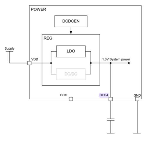
The nRF52840’s exposed power rails are:
- DEC1: 0.9 V regulator digital supply decoupling
- DEC2: 1.3 V regulator supply decoupling (Radio supply)
- DEC3: Power supply decoupling
- DEC4: 1.3 V regulator supply decoupling. Input from DC/DC regulator. Output from 1.3 V LDO
I set up to apply the glitch to DEC1. Looking at the pin’s role, this makes sense. DEC1, at 0.9V, is the lowest-voltage rail and likely powers the core, where code execution happens. Glitching here has a better shot at disrupting instructions, like those checking APPROTECT, and is less likely to be smoothed out by other regulators.
Board Modifications Link to heading
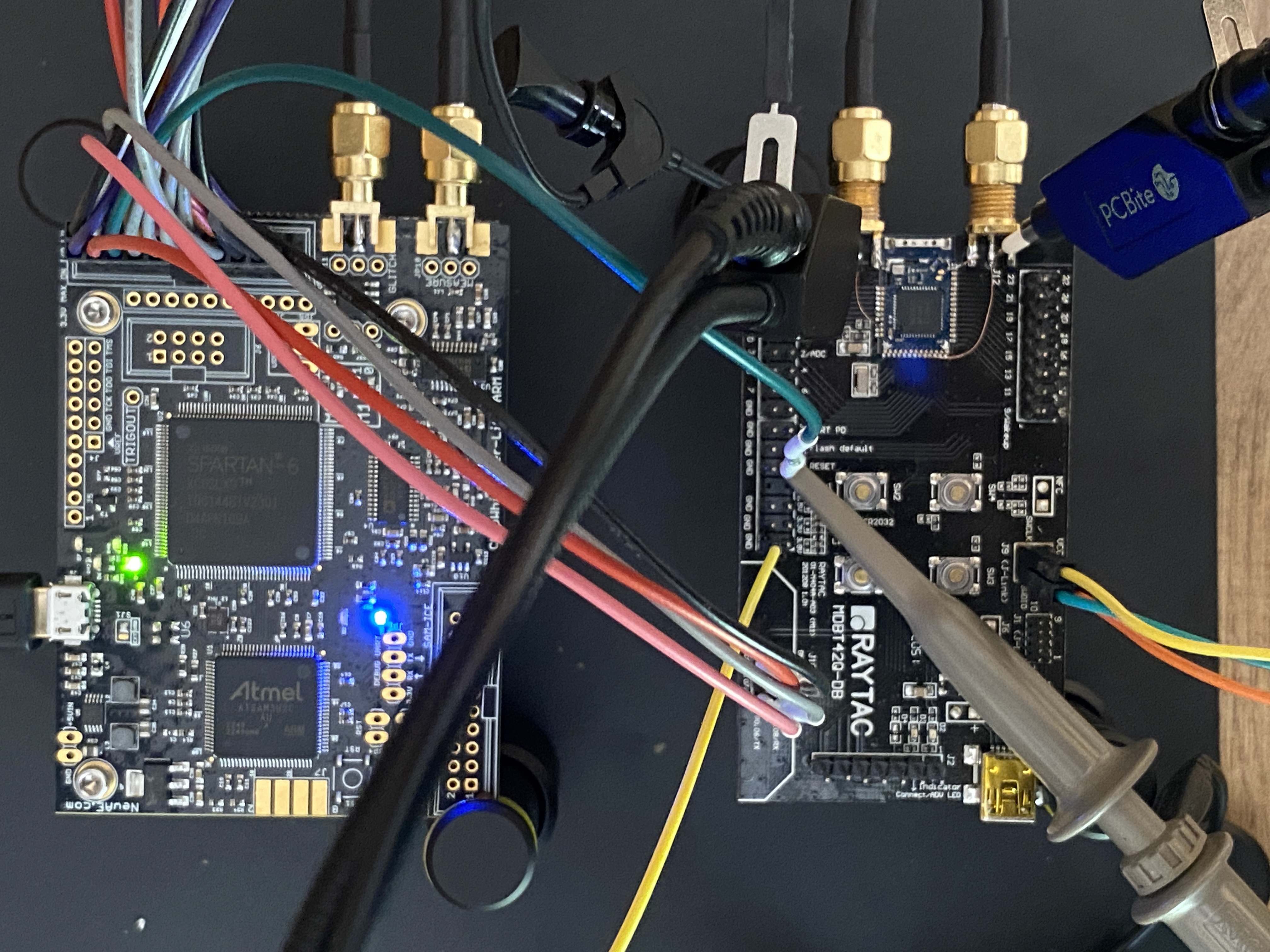
To insert the ‘shorts’, I used a Chipwhisperer Lite, a very handy and flexible tool for these kinds of tasks.
I had to make a few modifications to the target development board:
- I removed two capacitors connected to DEC4 and soldered this pin to an SMA1 connector. This point was used to measure the chip’s power consumption during execution (see the next section). Removing the capacitors reduced their ability to smooth out voltage variations, allowing me to capture more distinct changes in power consumption.
- I soldered an SMA1 connector to DEC1 to inject the glitch.

This setup made it easier to get consistent results, which is key for tweaking the attack.
Capturing Power Traces Link to heading
Next, I needed to determine when to insert the glitch. We can narrow down the window to the ‘boot’ time, as that’s likely when APPROTECT is read. But how long is the boot process?
Ideally, you’d flash a simple program that sets an I/O pin high after boot and measure the time from reset to that event. But my chip is locked, so no new firmware :/. Instead, I figured I could use power traces to get a sense of what’s happening.
What are power traces? You might think a chip uses steady power, with spikes only for heavy tasks like wireless. Not quite. Power consumption changes a lot depending on the instructions being executed. By measuring this, you can get clues about what the chip’s doing.
The firmware flashed on the chip on the development board first does some basic initialization, then loops waiting for serial input. So I expect some variation during boot and a steady pattern in the idle loop.
If I capture a power trace from reset, I should see varying power use during boot, then a steady, repetitive pattern when it hits the idle loop. The time from reset to that steady pattern is the boot time—likely when APPROTECT gets configured.
This sounds straightforward, but it’s tricky because of scale. Zoom out too far, and the trace looks flat. Zoom in too much, and it’s all noise. Finding the right view is a hassle.
To measure the power traces, I connected the ADC from ChipWhisperer to DEC3, with the decoupling capacitor removed.
def capture_and_plot():
    # Power off target, arm, power on
    scope.io.target_pwr = False
    time.sleep(.5)
    scope.arm()
    scope.io.target_pwr = True

    # Retrieve the trace
    ret = scope.capture()
    trace = scope.get_last_trace()
    [...]
    plot code here
    [...]
See the full notebook for more details.
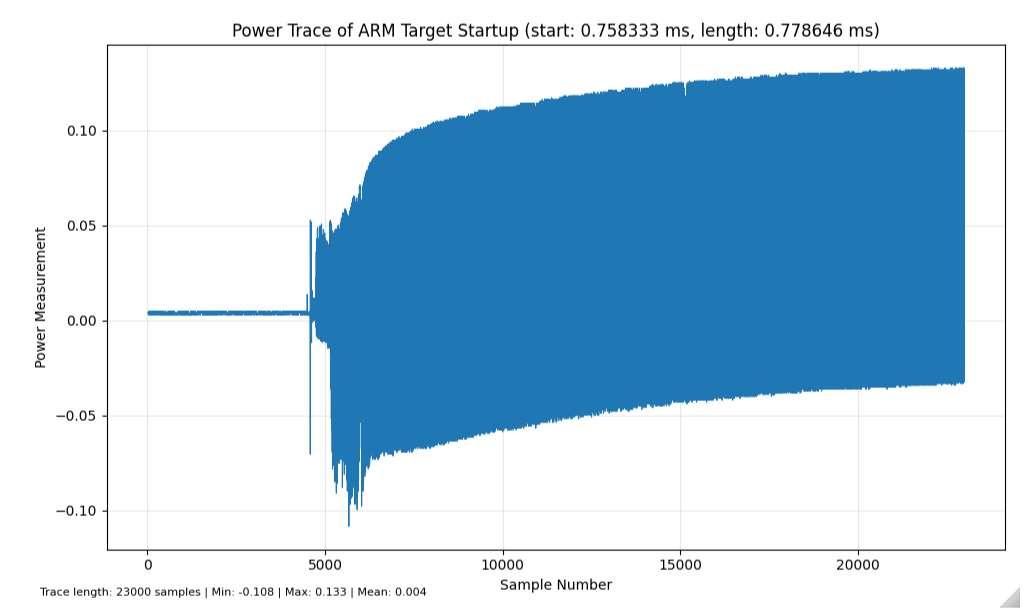
- I started by capturing the first 7 ms after reset and plotted the results.
For this, I configured the ChipWhisperer ADC to capture as many samples as possible (23K; 24K is the max, afaik). I set the offset to 0, to start capturing as soon as the trigger was triggered. The trigger was the rising edge of the reset line (hooked to the ChipWhisperer), so the capture would start as early as possible. The clock was set to the lowest value I could without ChipWhisperer complaining—3.2 MHz and clkgen_x1 as adc_src. This was intended to capture as wide a signal as possible, zoomed out.
%matplotlib widget
import matplotlib.pyplot as plt
import time

# Configure
scope.gain.gain = 4
scope.adc.samples = 23000
scope.adc.offset = 0
scope.clock.clkgen_freq = 3.2E6
scope.clock.adc_src = "clkgen_x1"
scope.trigger.triggers = "nrst"
scope.adc.basic_mode = "rising_edge"
scope.io.hs2 = "clkgen"

capture_and_plot()
The result can be seen in the following image:
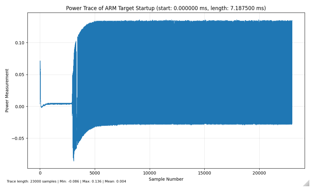
From this trace, I could differentiate the following ‘sections’:
- Initial Noise (0–0.5 ms): Some odd behavior at the start. Power supply stabilizing?
- Low-Power Phase (0.5–2 ms): Minimal consumption, maybe early boot stages?
- Steady Pattern (2–7 ms): Power increases and settles into a repetitive pattern, which I’m guessing is the idle loop.
On the previous plot, the initialization section seems to be somewhere between sample 3K and 5K.
This time, I increased the clock frequency to the max, set the adc clock source to clkgen_x4 for best resolution, and moved the offset to target around what was sample 3K on the previous plot.
%matplotlib widget
import matplotlib.pyplot as plt
import time

# Configure
scope.gain.gain = 4
scope.adc.samples = 23000
scope.adc.offset = 2800 * 2 * 4
scope.clock.clkgen_freq = 7.3828E6
scope.clock.adc_src = "clkgen_x4"
scope.trigger.triggers = "nrst"
scope.adc.basic_mode = "rising_edge"
scope.io.hs2 = "clkgen"

capture_and_plot()
The result can be seen below:
The capture is now much more focused, and we can see that what looked like a steady start is actually several sections. There’s some variation early on, probably the end of initialization, then it stabilizes but keeps rising slightly. I’m not sure why the “stable” part rises—could be voltage scaling, a background task, or maybe my probe drifting. Let’s try to zoom in again a little more, and move the offset to try to get the start of the variations on the signal:
%matplotlib widget
import matplotlib.pyplot as plt
import time

# Configure
scope.gain.gain = 4
scope.adc.samples = 2500
scope.adc.offset = 2800 * 2 * 4  + 4500
scope.adc.basic_mode = "rising_edge"
scope.clock.clkgen_freq = 7.3828E6
scope.clock.adc_src = "clkgen_x4"
scope.trigger.triggers = "nrst"
scope.adc.basic_mode = "rising_edge"
scope.io.hs2 = "clkgen"

capture_and_plot()
The result looks promising:
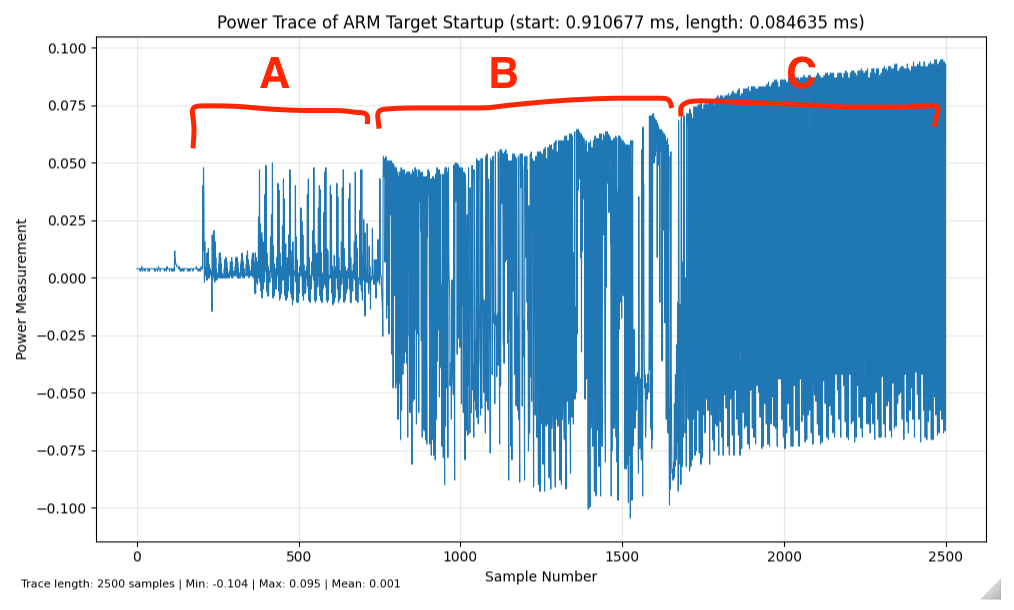
Three clear phases stand out:
- Phase A (Low Peaks, ~0.5–1.5 ms): Sporadic low-power activity, likely early boot (e.g., bootloader or ROM code).
- Phase B (High, Uneven, ~1.5–3 ms): Higher power but inconsistent, probably initialization tasks like setting up peripherals or APPROTECT.
- Phase C (Uniform High, ~3 ms onward): A consistent, repetitive pattern, matching the idle loop.
Glitching from 0.5 ms up to 4 ms should cover the whole boot process.
Injecting a Glitch Link to heading
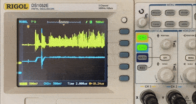
At this point, most of the heavy lifting was done. The only thing I added to the setup was connecting the scope to see what was going on—specifically, to check if I was injecting the glitch where I intended.
In the image below, CH1 (yellow) is the voltage at DEC4, and CH2 (pale blue) is the voltage at DEC1. In CH2, it’s easy to see the glitch being inserted at different points in time, incrementally shifting to the right. The scope’s trigger input was connected to the reset pin, which went high when the board was powered on by the ChipWhisperer.
Finding the Correct Parameters Link to heading
At this point, the process feels like a mix of black magic, trial and error, hope, and occasional despair. Nothing works until, suddenly, it does. When it fails, you’re left wondering if you messed up, if a connection is faulty, if the IC isn’t vulnerable, or if the glitch is too weak, too strong, too early, too late, too short, or too long.
You can follow a methodology to reduce some of the guesswork—I recommend checking out The Hardware Hacking Handbook—but there’s still a lot of uncertainty in the process.
After many tests, I finally succeeded. Or so I thought… (more on that later).
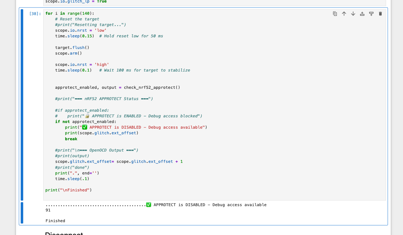
The image above shows a loop that powered the target device on and off while incrementing the ext_offset value each time. This value sets the number of clock cycles the ChipWhisperer waits after the trigger input (the reset line in my setup) before injecting the glitch.
After each iteration, the Python code ran check_nrf52_approtect(), which connected to the nRF52840 and used string-matching to check if APPROTECT was still enabled, based on results from earlier tests.
Now to the Real Device Link to heading
In theory, the next steps were simple: 1) remove the IC from the development board, 2) remove the victim IC from the device, 3) solder the victim IC onto the development board, and 4) repeat the attack.
But step 1 went wrong fast. While desoldering the IC and holding it with tweezers, I bumped it, knocking off two capacitors and an inductor from the board. I managed to resolder the inductor, but the capacitors—tiny 0.6mm x 0.3mm components—vanished under mysterious circumstances … don’t ask …
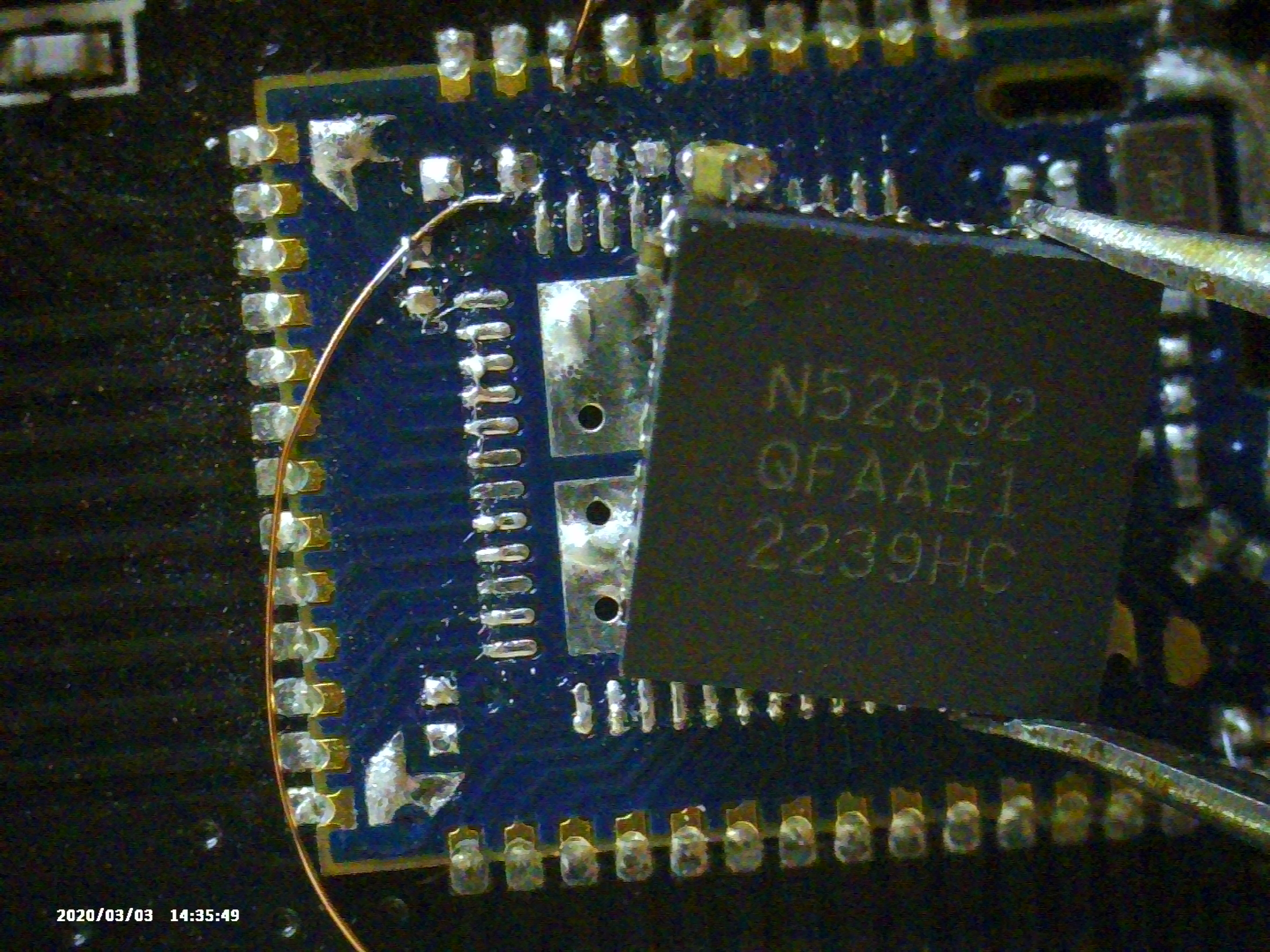
Soldering the victim nRF52840 from the target device onto the development board was another challenge. Let’s call it a nightmare. My QFN soldering skills need work.
After I was done soldering, the debug probe couldn’t even connect to the IC.
See the image below—can you spot the problem?
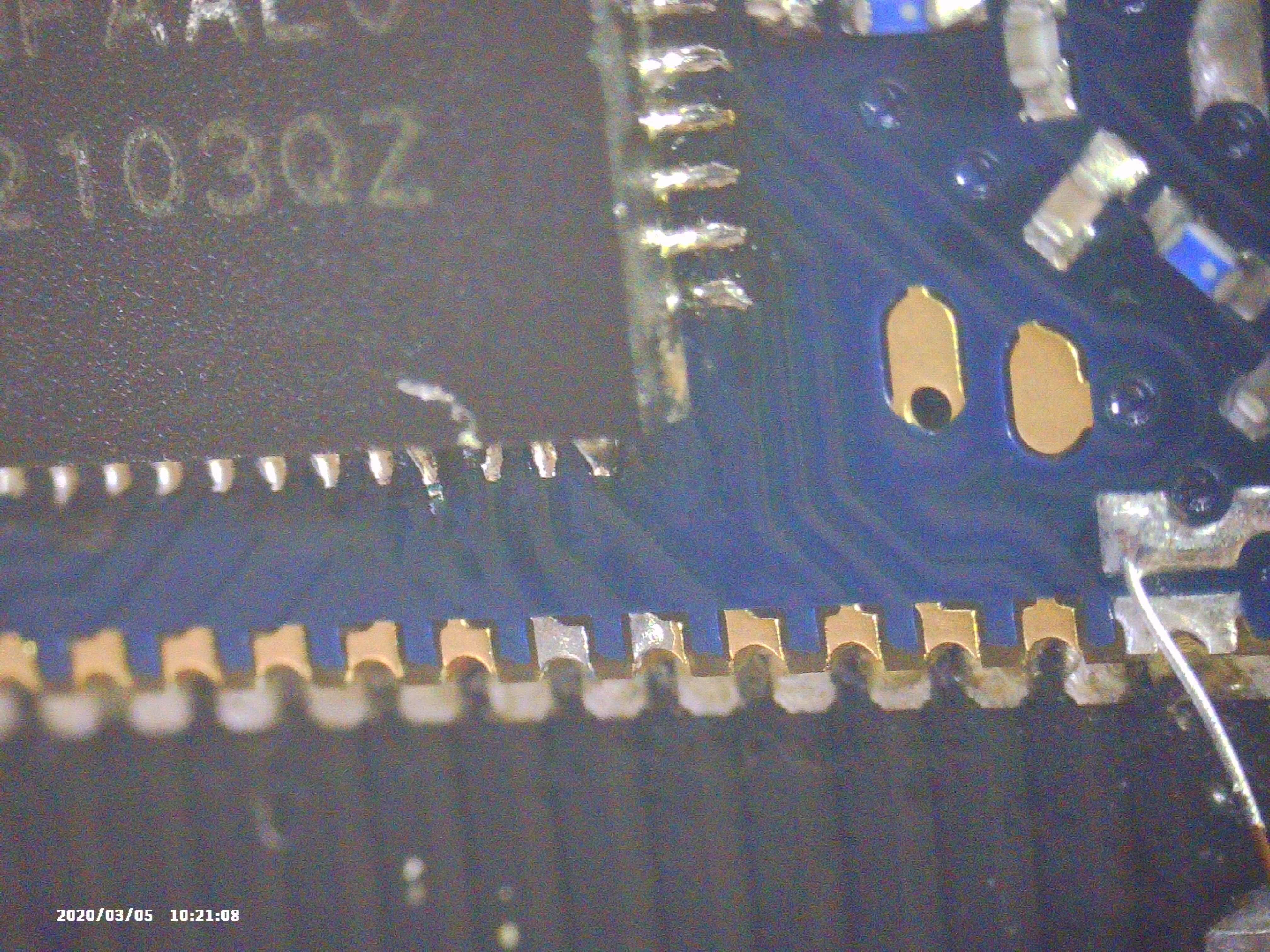
In the vertical row of solder joints, the bottom one isn’t making contact. And it’s SWDCLK, of course.
This is where working methodically and documenting earlier steps paid off. After these unexpected board modifications and not-so-great soldering, it was hard to pinpoint what was failing.
After fixing the bad solder joints and rerunning the experiment, I finally got the “Success” message!
But when I tried to dump the memory, it failed again. I don’t recall the exact error message, but OpenOCD launched fine, I could telnet to the server on port 4444, yet reading the memory didn’t work. I wasn’t sure what was wrong. Worse, I realized I hadn’t tried dumping the memory with the unlocked IC earlier, so I had no baseline to compare against.
By this point, I had a JLink adapter, so I tested with that and the STLinkV2. No luck.
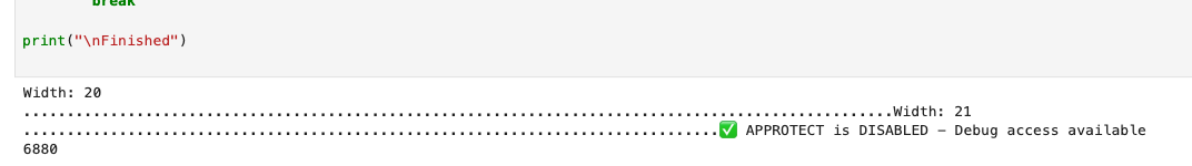
After a lot of effort, I started suspecting the glitch was leaving the IC in a strange state—one where the OpenOCD initialization phase worked, and my script detected it as ‘unlocked’, but it wasn’t functional enough to actually allow reading the register. So I started to test again with different glitch parameters. This time, I iterated over different glitch widths, not just locations.
And finally: SUCCESS!
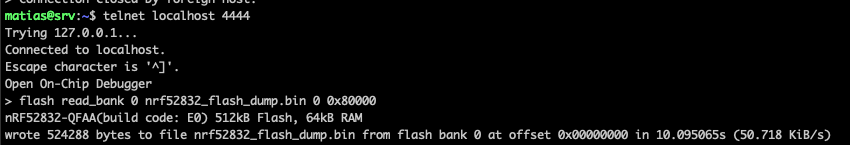
I revised the validation function to verify a successful memory chunk read, reporting success only when the read operation was confirmed. Upon achieving a positive result, I dumped the entire firmware using the command flash read_bank 0 nrf52832_flash_dump.bin 0 0x80000, as illustrated in the image below.
Final Notes Link to heading
This project was way messier than it sounds here—a mix of trial, error, and occasional despair. The cover image, clearly a photo-op, my desk was a mess. Persistence and breaking things down step by step were crucial, but I also learned some hard lessons that might save you trouble.
First, don’t trust OpenOCD’s messages alone to confirm APPROTECT is disabled. My initial “success” was misleading because I only checked if the debugger connected, not if I could actually read memory. Later, I found the chip was in a weird state—unlocked enough to connect but not functional for dumping firmware. Always validate by trying to read a small chunk of memory (like with OpenOCD’s mdw command) to confirm the chip is fully accessible.
Second, don’t underestimate resoldering ICs. Swapping the nRF52840 onto the development board sounded simple, but my shaky QFN soldering skills turned it into a nightmare. A bad SWDCLK connection cost me hours of debugging, and knocking off tiny capacitors was a disaster.
Finally, document everything. My notes on OpenOCD outputs and power traces were a lifesaver when things went wrong, like after the soldering fiasco. Without them, I’d have been lost trying to figure out if the glitch, the board, or my setup was the problem.
You can find my Jupyter notebooks for the voltage analysis and final glitch setup here. If you’ve tackled a similar project or hit your own roadblocks, I’d love to hear what worked for you—reach out!
Previous Work Link to heading
Here are the main resources I used for this experiment:
- https://limitedresults.com/2020/06/nrf52-debug-resurrection-approtect-bypass/
- https://limitedresults.com/2020/06/nrf52-debug-resurrection-approtect-bypass-part-2/
- https://i.blackhat.com/eu-20/Wednesday/eu-20-LimitedResults-Debug-Resurrection-On-nRF52-Series.pdf
- https://limitedresults.com/2021/03/the-pocketglitcher/
- https://docs.nordicsemi.com/bundle/IN/resource/in_133_v1.0.pdf
- https://diary-of-a-wimpy-researcher.org/posts/oculus2-controller-extracting-fw/
- https://github.com/atc1441/ESP32_nRF52_SWD
- https://nostarch.com/hardwarehacking
ANNEX Link to heading
Enabling/Disabling APPROTECT Link to heading
To enable APPROTECT on my development board’s chip, which comes unlocked from the factory I connected the debugger probe, used Telnet to connect to port 4444, and wrote the value 0xFFFFFF00 to the APPROTECT UICR register:
halt target halted due to debug-request, current mode: Handler PendSV xPSR: 0x0100000e pc: 0x0002ae7e msp: 0x2000ff84
flash fillw 0x10001208 0xFFFFFF00 0x01 wrote 4 bytes to 0x10001208 in 0.063454s (0.062 KiB/s)
reset
I quickly learned that once APPROTECT is enabled, disabling it isn’t straightforward. When I initially connected with OpenOCD and my STLinkV2 probe, I got this warning, which I completely ignored:
nRF52 device has a CTRL-AP dedicated to recover the device from AP lock. A high level adapter (like a ST-Link) you are currently using cannot accessthe CTRL-AP so ’nrf52_recover’ command will not work. Do not enable UICR APPROTECT.
This was OpenOCD warning me not to enable APPROTECT, as I wouldn’t be able to disable it. And that’s exactly what happened. I ended up with a locked nRF52840. I hadn’t realized there are different types of debug probes—it’s not just “official” vs. “clone.”
JLink vs ST-Link V2 Link to heading
There are “high level” and “low level” debug probes. ST-Link V2 is high level and can only talk to the AHB-AP, whereas J-Link can talk to AHB-AP as well as CTRL-AP. Disabling APPROTECT involves a mass erase via the CTRL-AP, accessible only by low-level adapters.
From the datasheet:
Access port protection is disabled by issuing an ERASEALL command via CTRL-AP. This command will erase the flash, UICR, and RAM, including UICR.APPROTECT. Erasing UICR will set UICR.APPROTECT value to Disabled
CTRL-AP - Control access port
The control access port (CTRL-AP) is a custom access port that enables control of the device when other access ports in the DAP are disabled by the access port protection.